What is a PCB? #
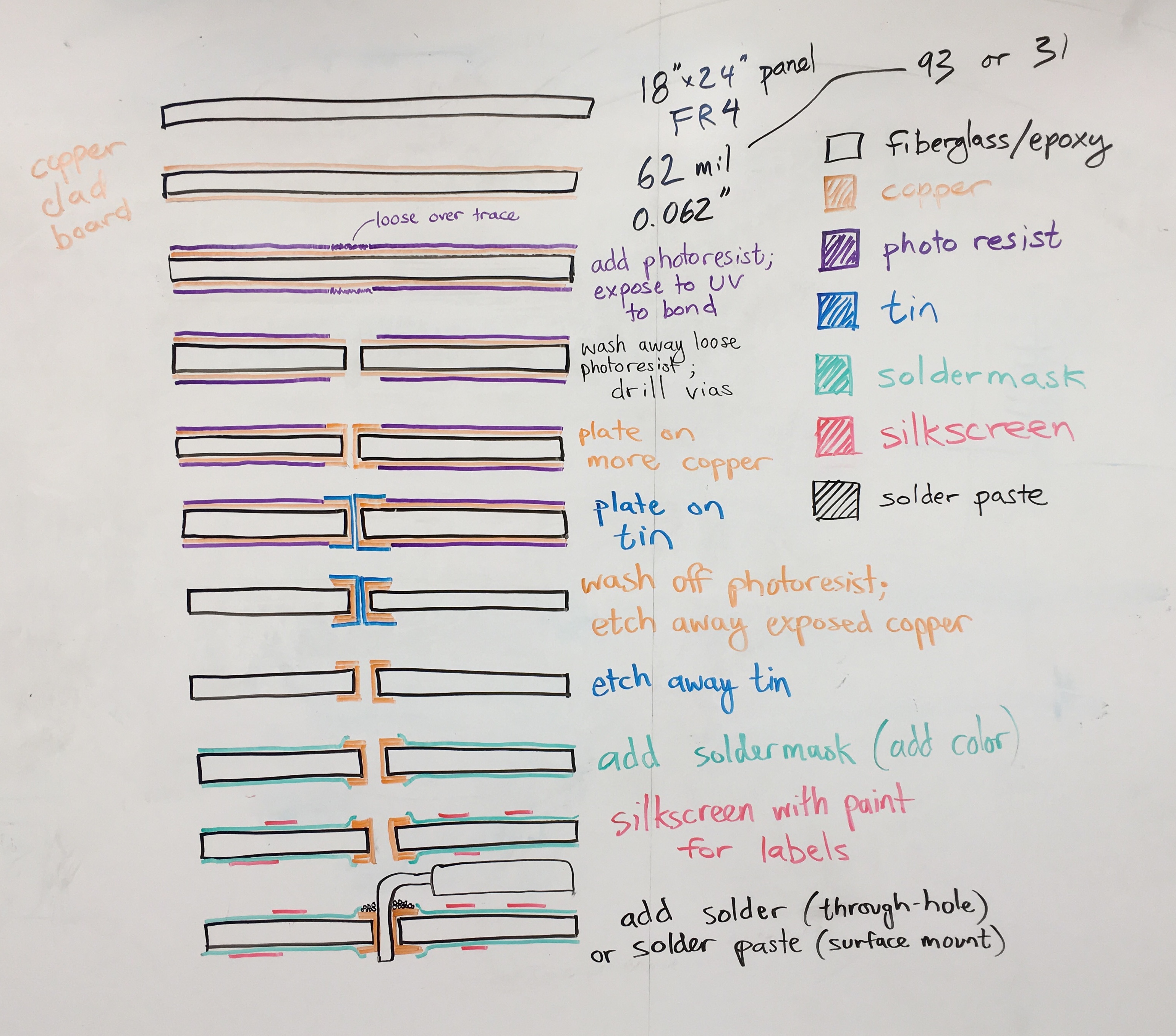
A PCB is a printed circuit board. Essentially, it consists of an insulated board coated with copper pathways that allow current to flow between components. The pathways are created by etching away from a complete coating of copper and by drilling copper-coated holes. The circuit components are then soldered to the board after it is produced.
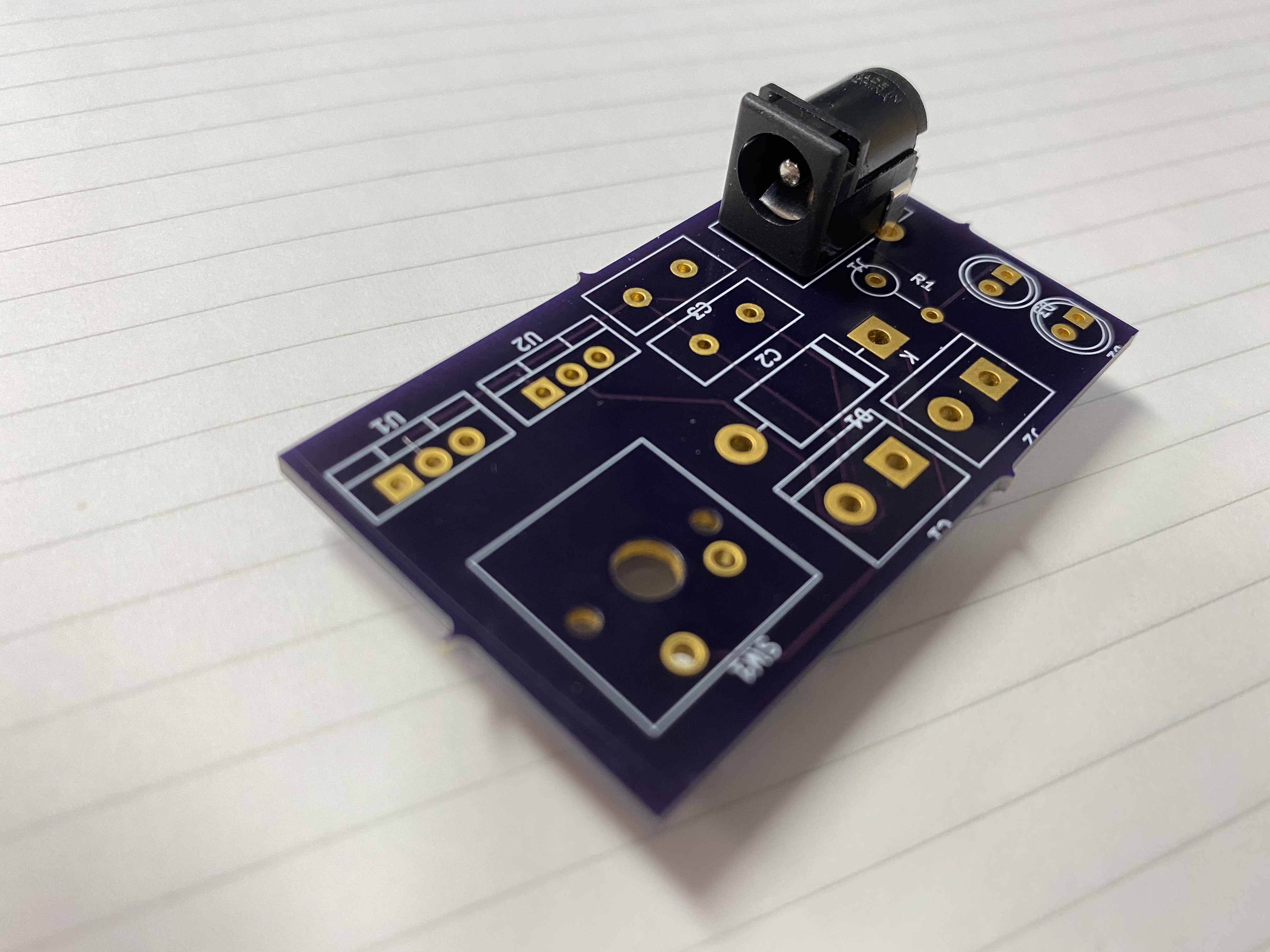 Here’s a purple PCB from OSHPark. Note that the power jack is oriented in such a way that the power cord would intersect with other parts on the board. This is the kind of detail that is really hard to get right on the first try.
Layers of a PCB #
What software? #
You should use Kicad. It’s free and open source, which means that once you learn to use it, you can make PCBs as long as you have a computer. You could also try Eagle, which might be a little easier to use, but it requires a subscription if you want to make a commercial board bigger than this chocolate bar that I’m eating. I’ve designed a few boards in Eagle; neither Kicad nor Eagle is great (though both are improving fairly quickly after a decade or so of stagnation). You could also try a browser-based program like Upverter, but if they shut down their servers, your designs are gone.
If it makes you feel any better, expensive PCB design software, like Altium Designer, is also pretty lousy. (I think the general problem the industry is facing is that electrical engineers are a relatively small population, and they’re pretty good at figuring out how to use bad software.)
Learning Kicad #
Here’s a rough summary of how to use Kicad.
Preparation Steps #
- Make sure you have a working breadboard prototype of your circuit.
- Draw a schematic diagram of your circuit on paper, so you know what you are trying to re-create on Kicad.
- Determine any physical constraints for your final printed circuit board: its ideal length and width, any components that need to be in a specific location (e.g., to match up with breadboard holes or allow for plug access).
- (If you’re using a laptop with a trackpad, plug in a real mouse.)
Steps with the Software #
- Open Kicad
- Make a new project.
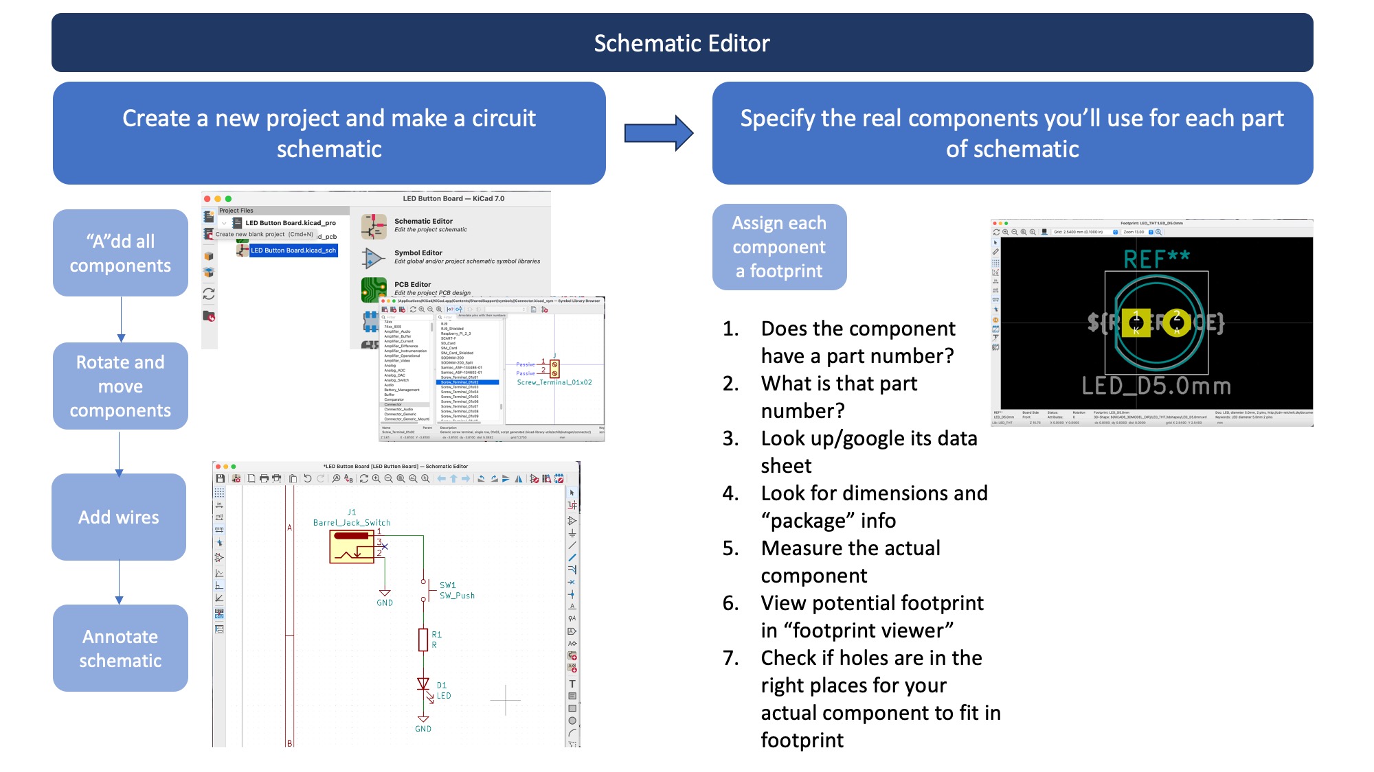
- Enter the Schematic Editor.
- Add components to the schematic file.
- Wire the components together in the schematic.
- Assign a footprint to each component (“Tools” menu).
- “Update PCB from Schematic” (“Tools” menu) to generate a netlist from the schematic.
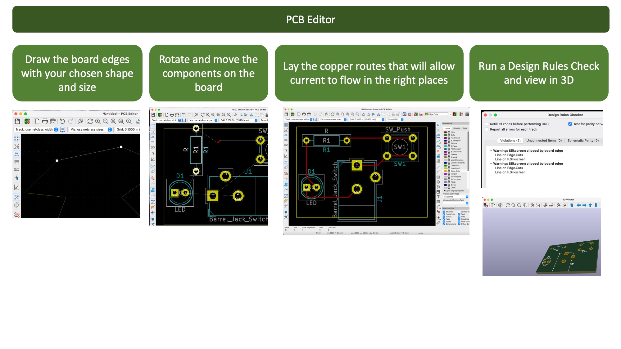
- Enter the PCB Editor.
- If your footprints are all in a stack, right-click > Global Spread and Place > Spread out All Footprints
- Make a mechanical outline of the PCB on the Edge.Cuts layer using “Add Graphic Line or Polygon.”
- Roughly arrange the parts the way you want them.
- Place mechanically critical components.
- Place the rest of the components and route traces between everything.
- Run a design rule check (DRC) from the “Inspect” menu.
- Repeat cycle: schematic/footprints -> gen. netlist -> read netlist -> tweak layout -> run DRC
- Submit .kicad_pcb file to OSH Park (or possibly generate Gerber files for another manufacturer).
Keyboard Shortcuts #
Tip: Use the KiCad “hot key keyboard shortcuts” to more easily move, rotate, and label components in your schematic and layout.
Overview of KiCad Workflow #
Tutorials to get you started #
- Chris Gammell’s video tutorial on Youtube
- Brian Bryce’s written tutorial
- Digikey’s Intro to KiCad playlist on Youtube
Note that the first two tutorials above were created before the latest version of KiCad was released, so a few aspects of your KiCad interface might look slightly different. The main steps remain the same, however. For the most up-to-date written tutorial, try KiCad’s own “Getting Started in KiCad”:
General PCB checklist (not applicable to every project) #
- Mounting holes
- Power and ground connector on board
- Connector pins labeled
- Pin labels not covered by connector bodies
- All designators legible, not obscured by vias, oriented the same way, if possible
- Power LED, if you can fit one
- Testpoints on critical lines, if pins too small to probe
- Two grounded holes (can be the same footprints used for connector pins) to solder in a wire loop for scope ground clip
- Date, project name, board revision number
- Protection circuitry on interfaces (overvoltage zeners, reverse polarity diodes)
- You did actually run a design rule check, right?
- No design rules “temporarily” loosened?
- Drill sizes in allowable range for manufacture
- Test upload files with manufacturer, if possible
PCB gallery #
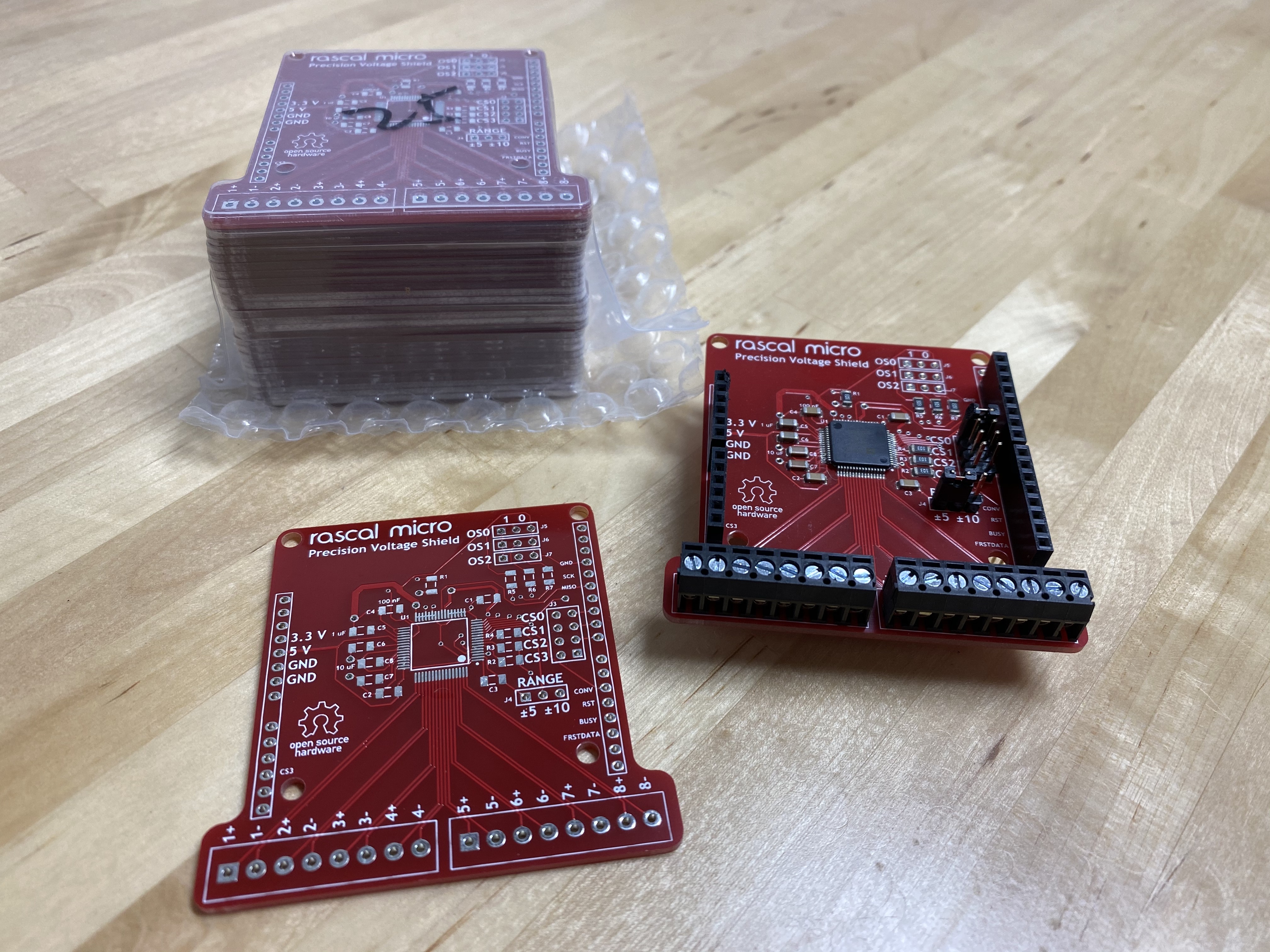 I (Brandon) used to run a company where I manufactured and sold these small Arduino shields. The shield turns your Arduino into an 8-channel voltmeter, and you can stack them to get more channels.
The shrink-wrapped pile is how the PCBs arrived from China, the empty PCB is before I soldered anything on, and the other device has all the components soldered on. Notice that the PCB is a mix of surface-mount (abbreviated SMT or SMD, for surface-mount device) and through-hole components. Today, surface-mount components are preferred for almost everything except connectors, where the strong mechanical connection to the PCB provided by the through-hole is valuable. But, for prototyping, SMT stuff is a nightmare.
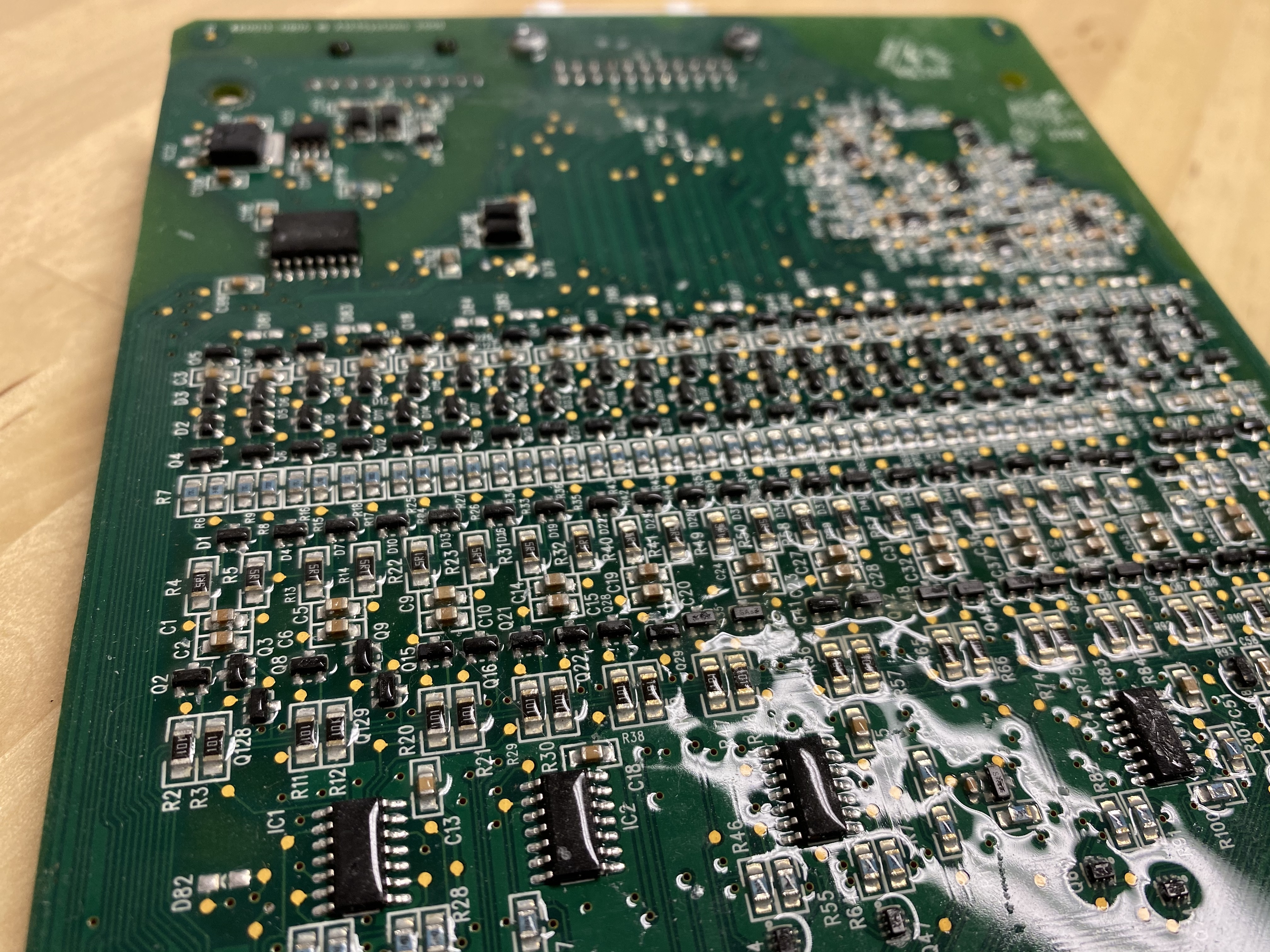 Speaking of nightmares, here’s an insane PCB from now-defunct battery manufacturer A123, formerly in Watertown, MA. The PCB is a charge controller from a huge battery pack; its job was to monitor every cell in the pack, and make sure that they were all charged equally and that none of them got too hot. Prototyping this was probably really difficult– I would bet they made smaller versions first to validate the circuit before they made the whole thing.
Note also that the PCB is covered in a conformal coating (AKA shiny goo). This is to protect the circuit from dust and moisture. Enough dirt and oil piling up on a PCB can make new, slightly conductive paths between pins, which can cause problems for some circuits.
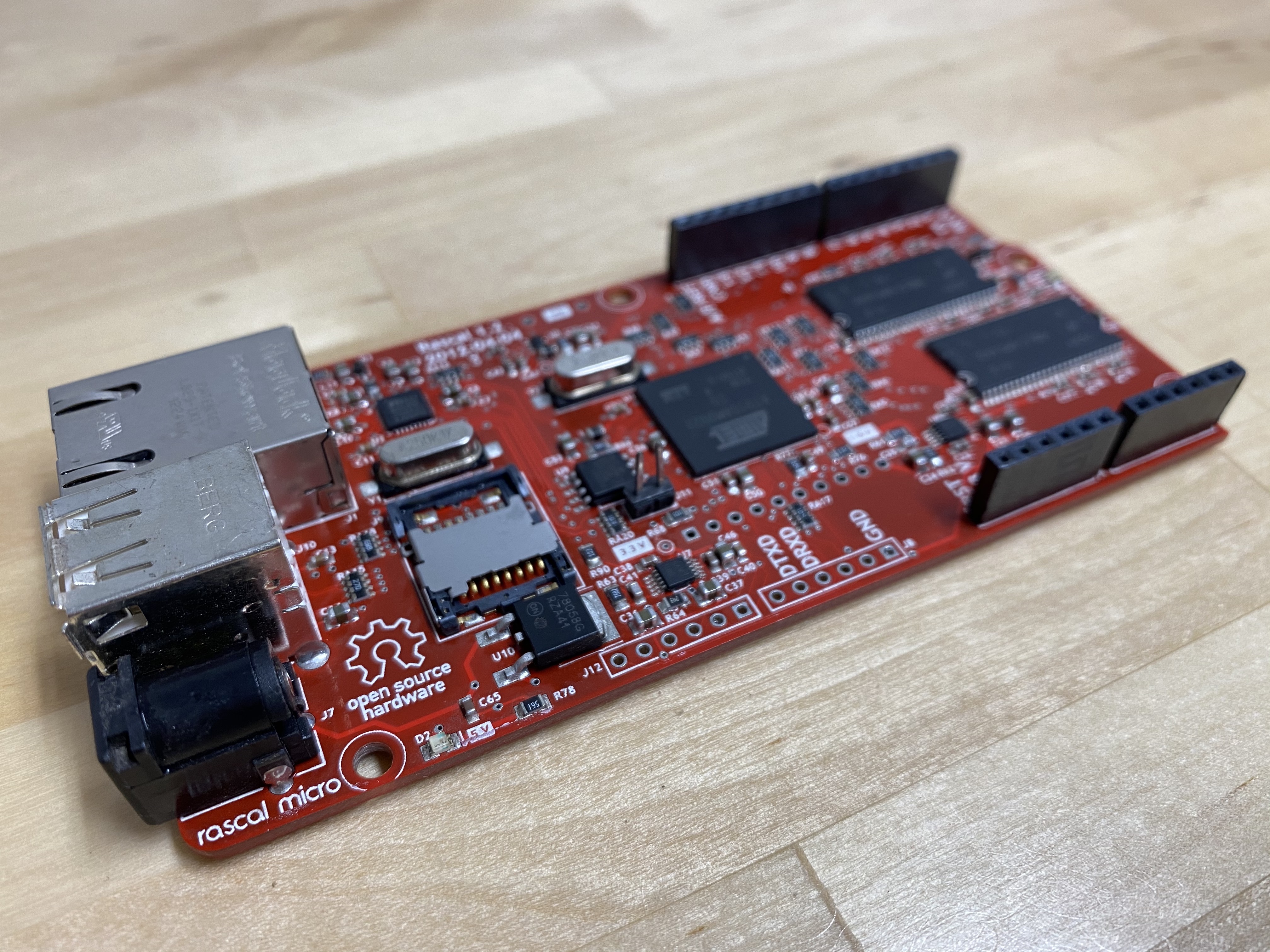 This PCB consumed six months of my life. It is the most complex engineering project I have ever completed. The central chip, an Atmel AT91SAM9G20 ARM processor running at 396 MHz, is a ball-grid array package, which means that there is a grid-shaped array of metal balls under the chip instead of pins around the outside. It is risky to solder this kind of chip yourself, because if you get solder blobs underneath shorting out pins, you can’t see them without an X-ray machine.
This PCB is also the only PCB I’ve worked on where the length of the traces mattered. The memory signals on the board are running at 133 MHz, so if one memory trace is a lot longer than another, the nanosecond differences in the time it takes for signals to propagate down the length of the trace mean that a clock cycle can end before all the signals arrive. In the case of this board, it meant that everything went fine, until you tried to do a particularly write-heavy operation (specifically, cloning a git repository) at which point, a signal would arrive late, so the CPU would find an invalid instruction in its memory and reset. I had to revise the board to make all the traces much closer to each other in length. I blogged about the details of this painful experience.
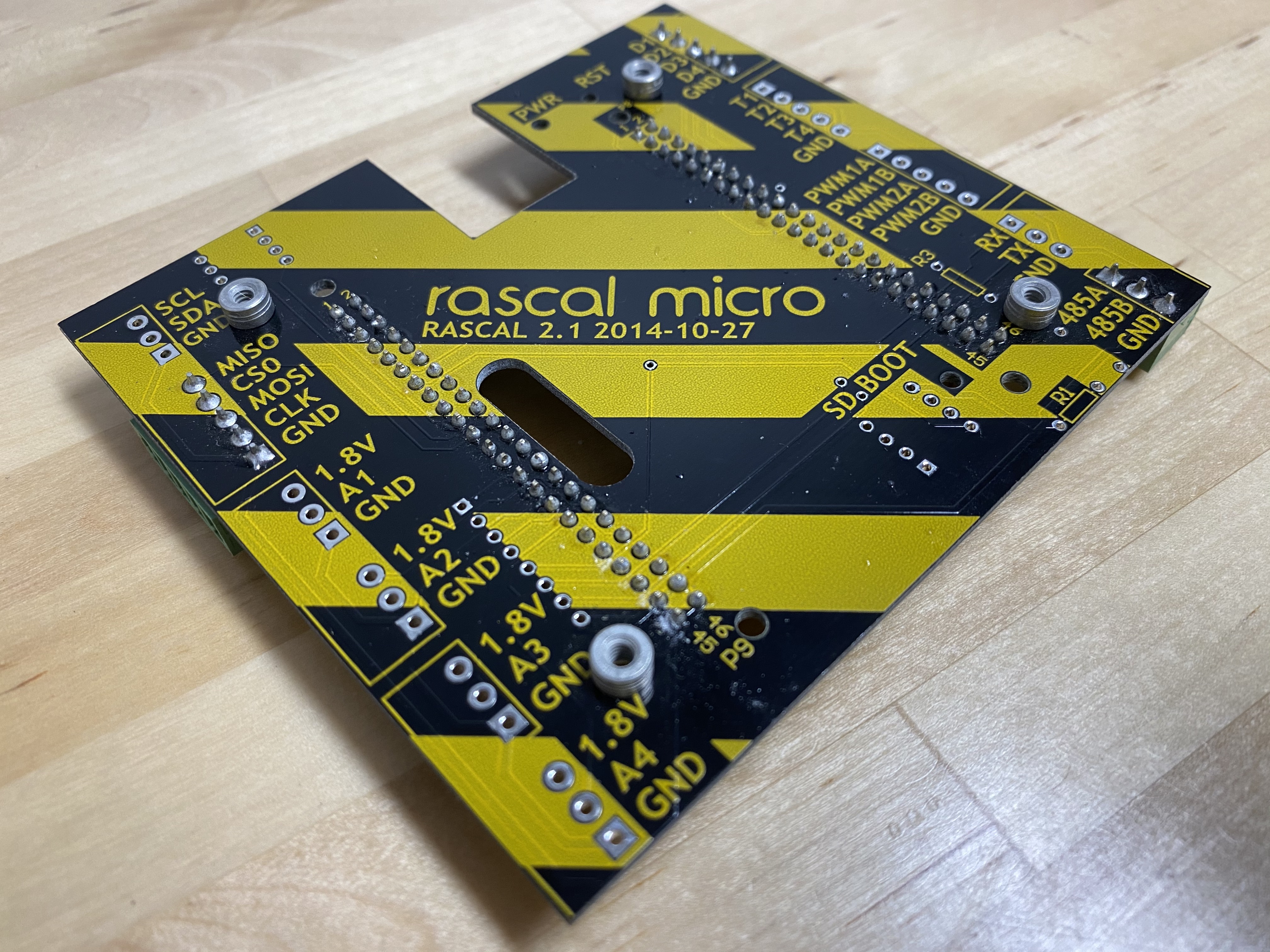 This PCB is cool just because I used black soldermask and yellow silkscreen to make it look cool, but no more expensive than any other board.
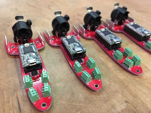
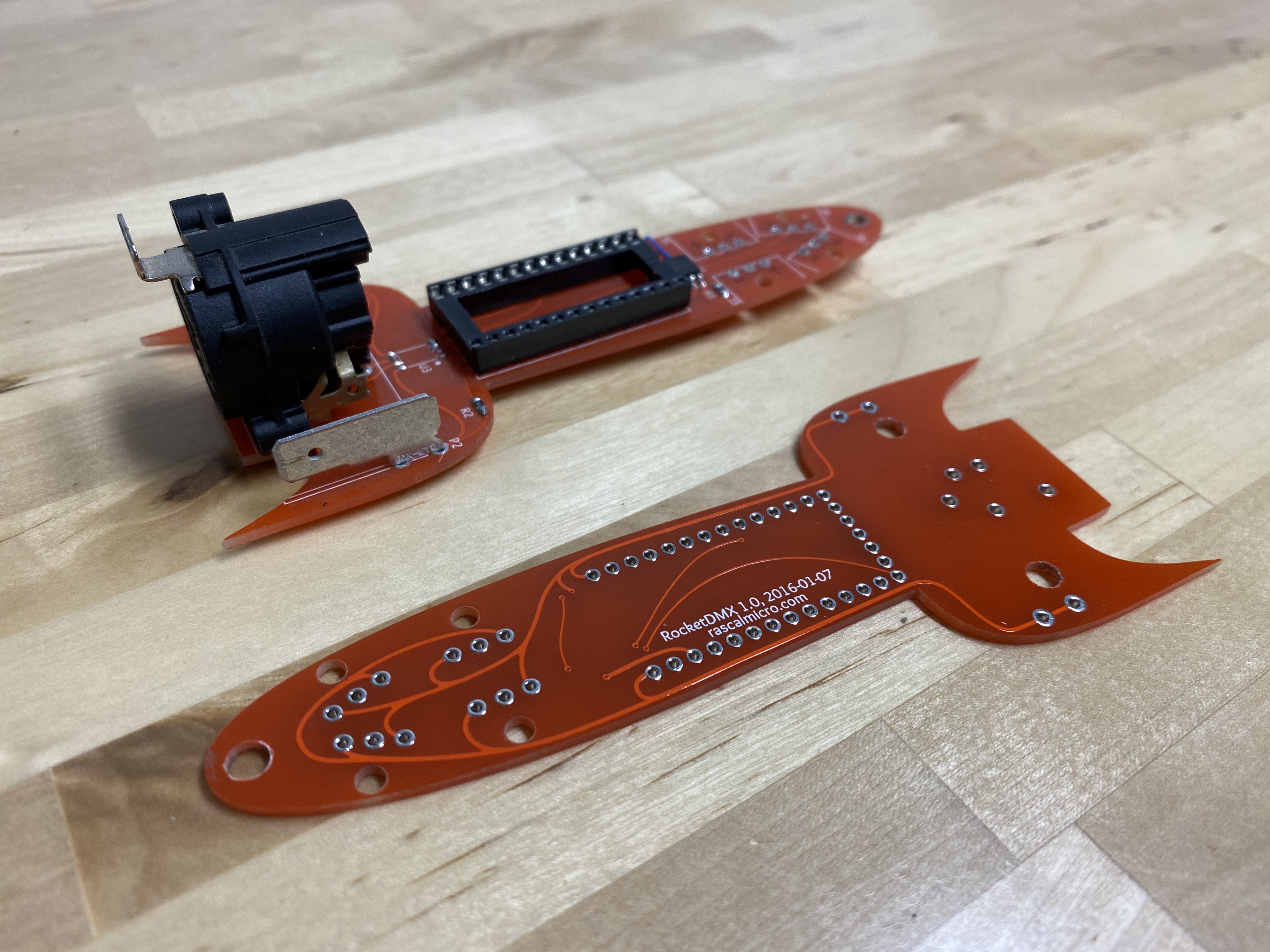 Here are some fanciful PCBs I made a few years ago. The rocket engine is actually a DMX connector; the thing is used to control stage lights. This is just to give you the idea that PCBs don’t just have to be boring rectangular things. I made this PCB using weird open-source software called PCBmodE: https://github.com/boldport/pcbmode. If you want to make a simple, but oddly shaped, PCB, maybe that would work for you.
PCB design tips from former ME 30 students #
Lessons learned from Gus, Emily, and Alex: #
- figuring out how to ground things
- the circuit doesn’t actually have to complete a circle
- realizing that the rats nest is a guide for how to lay your traces
- you can use any footprint that fits your component
- how to lay components in series vs. parallel in the schematic
From Ronan, Teddy, Majeed, Matias: #
- Finding footprints was very time consuming
- KiCAD schematic is mainly symbolic not functional (not for running a simulation)
- Difficult UI on KiCAD
- Learning keyboard shortcuts for KiCAD was useful
- Sometimes you need to go online to get footprints for parts not on KiCAD
- You can trace on both sides of the board - there are two layers
- Datasheets were a very useful resource
- YouTube is an amazing resource
- A solid understanding of the circuit schematic helped with the production of the PCB later on
From Jake, Charvady, Alanna, and Trevor: #
- Completely new software to all of us - all developed a basic understanding after P1
- All thought kicad was easy-to-use after the learning curve.
- Demo video was really helpful
- Updating libraries was hard to figure out and not explicitly clear at all
- Assigning the footprints and making sure you had the correct one. Flipping back between all datasheets
- Going back to circuit diagram and being able to update PCB layout directly.
- All the different layers of the PCB board and deciding which layer is used for what - 2 copper wire layers, top & bottom silk screen.
- Making sure things were facing in the right direction - barrel jack.
- Always had to be thinking of overall PCB layout - wiring and placing components.
- What to label. When in doubt, label everything.
- Where to place connector pins and how to connect in circuit diagram.
From other groups: #
- Troubleshooting issues: close the whole application and restart (“brain refresh”)
- Finding components: google main header, some are named weirdly
- Using a mouse instead of a trackpad
- Making schematic traceable and obvious, including labels, etc.
- Use ground symbols instead of connecting things to ground itself
- Don’t want overlap traces in contact
- Learn shortcut keys (example shift + M to move a component)
- Start by building it in a large area, and once you get the hang of it start minimize the area
- If components start to heat up, something is wired wrong
- Good practice: check all the wiring before you plug your circuit into a power source
- How to look up all the components of the circuit in the library
- Using the 3D viewer
- Placing wires on top and bottom layer
- Condensing components
- Kicad makes suggestions based on schematic
- Labeling pcb board on silk screen
- Using hot keys (M, R, E, etc.)
- Placing what you want to plug other things into in an easily accessible spot